 English
What is the working principle of pcb multilayer board?
What is the working principle of pcb multilayer board?
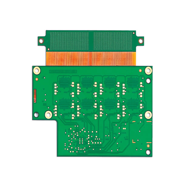
What is the working principle of pcb multilayer board? PCB multilayer board refers to the multilayer circuit board used in electrical products. Multilayer boards use more single-sided or double-sided wiring boards. A printed circuit board with one double-sided as the inner layer and two single-sided as the outer layer, or two double-sided as the inner layer and two single-sided as the outer layer, alternately connected by a positioning system and an insulating adhesive material Together, the conductive patterns are connected to each other according to the design requirements to become four-layer and six-layer printed circuit boards, also known as multi-layer printed circuit boards. Today, Xiaobian contacted the professional and technical personnel of Ucreate to introduce the working principle of PCB multilayer board.
With the continuous development of SMT (Surface Mount Technology) and the continuous introduction of a new generation of SMD (Surface Mount Devices), such as QFP, QFN, CSP, BGA (especially MBGA), electronic products are more intelligent and miniaturized, so It has promoted the major reform and progress of PCB industry technology. Since IBM first successfully developed a high-density multilayer board (SLC) in 1991, major groups in various countries have also successively developed a variety of high-density interconnect (HDI) microplates.
With the rapid development of these processing technologies, PCB design is gradually developing towards multi-layer and high-density wiring. Multilayer printed boards are widely used in the production of electronic products due to their flexible design, stable and reliable electrical performance and superior economic performance.
The biggest difference between PCB multilayer boards and single boards and double boards is the addition of internal power layers (maintaining internal power layers) and ground layers. Power and ground nets are primarily routed on the power plane. However, multilayer board routing is primarily based on the top and bottom layers, supplemented by intermediate routing layers. Therefore, the design method of multi-layer boards is basically the same as that of double-sided boards. The key is how to optimize the wiring of the internal electrical layers, so that the wiring of the circuit board is more reasonable and the electromagnetic compatibility is better.
The above is a detailed introduction to the working principle of pcb multi-layer board, I hope it can help you!
